
- Quartz Wafer
- Quartz wafer는 높은 작업온도, 높은 항부식, 양호한 열전도율, 높은 광투과율과 같은 많은 독특한 특징을 가지고 있으며,
이 특징들은 Quartz 웨이퍼를 반도체, 포토마스크, 마이크로파 필터, 광섬유 응용에 사용되고 있다.
Quartz Wafer Available
| High working temperature | High optical transmission |
| High stability | High anti corrosion |
| Good thermal conductivity | low dielectric loss |
| Stable dielectric constant | Superior mechanical properties |
What's differences ?
| Fused silica wafer ( Synthetic silica ) | Fused quartz wafer ( Natual silica ) |
| High OH content >1200 | Low OH content > 150 |
| Higher transmission in the UV range | Lower transmission in the UV range |
| Free bubbles and inclusions | Contain bubbles and inclusions |
| Very low fluorescence | High fluorescence |
| Impurity 5 ppm | Impurity 20 ~ 40 ppm |
Quartz Wafer Properties
| Chemical formula | SiO2 |
| Mechanical Properties | |
| Density | 2.2 g / cm3 |
| Poisson's ratio | 0.14 ~ 0.17 |
| Young's modulus | 72000 Mpa |
| Rigidity modulus | 31000 Mpa |
| Moh's hardness | 5.5 ~ 6.5 |
| Thermal Properties | |
| Transformation point | 1120 °C |
| Softening point | 1680 °C |
| Specific heat ( 20 ~ 350 °C ) | 670 J / kg °C |
| Thermal conductivity ( 20 °C ) | 1.4 W / m °C |
| Thermal expansion coefficient | 5.5×10 -7 cm / cm °C |
| Electrical Properties | |
| Resistivity | 7E7 ohm-cm |
| Insulating strength | 250 ~ 400 Kv / cm |
| Dielectric constant e | 3.7~ 3.9 |
| Dielectric absorption coefficient. | < 4E4 |
| Dielectric waste coefficient. | < 1E4 |
| Optical Properties | |
| Refractive index ( @ 589 nm ) | Nd =1.4584 |
Product Specification
| Growth | CVD / Oxy-Hydrogen melting / electric melting |
| Diameter | Ø 1" / Ø 2" / Ø 3" / Ø 4"/ Ø 6" / Ø 8"/ Ø 12" |
| Size | 10 x 10 / 20 x 20 / 50 x 50 / 100 x 100 / 200 x 200 mm |
| Thickness | 0.4 mm / 0.5 mm / 0.7 mm / 1 mm |
| Surface | one side polished / two sides polished |
| Flat | SEMI.Std. flat or Notch |
| TTV | <= 15 um |
| Roughness | Ra <= 10 A |
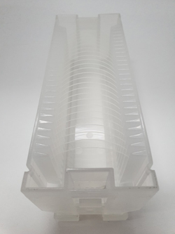
| Package | Ampak cassette / jar |